
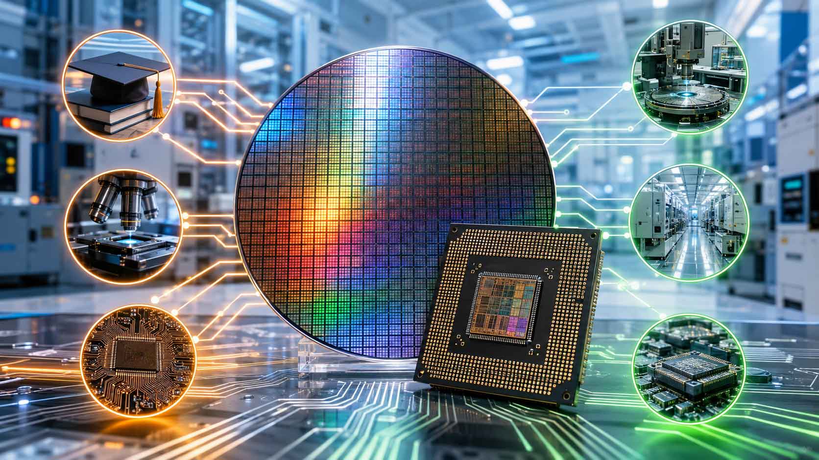
India is expanding its semiconductor workforce across chip design, fabrication, process engineering and advanced packaging as it develops capabilities across the entire semiconductor value chain.
The Ministry of Electronics and Information Technology said on July 30, 2026, that the government had adopted a multi-pronged talent-development roadmap under the Semicon India Programme and the recently approved Semicon 2.0.
The strategy combines specialised academic curricula, access to professional chip-design tools, manufacturing laboratories, industry-linked training and international academic partnerships. It covers semiconductor design and fabrication as well as assembly, testing, marking and packaging, commonly known as ATMP.
The information was submitted to the Lok Sabha by Union Minister of State for Electronics and Information Technology Jitin Prasada on July 29, 2026.
More than one lakh engineers trained through SMART Lab
The Skilled Manpower Advanced Research and Training, or SMART, Lab at the National Institute of Electronics and Information Technology in Calicut was established with the target of training one lakh engineers.
Its programmes cover very-large-scale integration, embedded systems and the Internet of Things. According to the government, more than one lakh candidates have now been trained through the initiative.
These fields support the development of semiconductors and electronic systems used in automobiles, telecommunications, industrial equipment, medical devices, consumer electronics and other technology-driven sectors.
Chips to Startup programme trains 68,000 people
India is also widening access to the specialised software and infrastructure required to design chips.
Under the Chips to Startup programme, participating educational institutions receive free access to advanced electronic design automation tools. These tools are used to design, simulate and verify semiconductor circuits before they are sent for manufacturing.
The government said usage of the tools had exceeded 24 million hours. Around 68,000 people have been trained through the programme, while 175 chip designs have reached the tape-out stage through the Semiconductor Laboratory in Mohali.
Tape-out is the stage at which a completed chip design is prepared for fabrication.
The programme enables students, researchers and participating institutions to undertake semiconductor design work using technologies employed across the chip industry.
Semiconductor studies introduced in engineering institutions
The government has also introduced semiconductor education more systematically into engineering institutions.
A committee comprising representatives from the semiconductor industry, academia and government prepared the Semicon India Future Skills Talent Committee Report, setting out a roadmap for developing India as a semiconductor talent base.
Following recommendations from the committee and MeitY, the All India Council for Technical Education introduced semiconductor curricula for undergraduate, diploma and minor-degree programmes.
The initiative is intended to create graduates with foundational knowledge relevant to chip design, electronics systems and semiconductor manufacturing.
Training expands from chip design to manufacturing
Alongside its established capabilities in semiconductor design and engineering, India is developing specialised skills required for fabrication, assembly, testing and packaging facilities.
MeitY has approved the establishment of a Semiconductor Assembly and ESD Training Laboratory at NIELIT Guwahati. The facility will provide training related to ATMP operations and support semiconductor manufacturing projects being developed in India’s northeastern region.
The India Semiconductor Mission has also partnered with semiconductor-equipment company Lam Research on a large-scale programme covering nanofabrication and process engineering.
The programme aims to train 60,000 people over ten years, adding to the workforce available for fabrication, ATMP and advanced-packaging operations.
These fields cover several stages through which semiconductor wafers and chips pass before they can be incorporated into electronic products.
Industry partnerships widen the training network
The government is connecting its talent-development programmes with semiconductor companies, training institutions and prospective manufacturing facilities.
FutureSkills Prime, implemented by MeitY in partnership with NASSCOM, offers online programmes for training, reskilling and upskilling in emerging technologies, including semiconductors.
An agreement between the India Semiconductor Mission and NAMTECH aims to train approximately 5,000 professionals over the next five years. It includes jointly endorsed certification programmes, faculty exchanges and international collaboration.
The partnership also covers student internships and apprenticeships at semiconductor fabrication plants, ATMP and outsourced semiconductor assembly and test facilities, and design companies supported by the mission.
Separately, an agreement with IBM provides for the establishment of a semiconductor research centre in India. Its areas of work will include research and development, intellectual-property sharing, chip prototyping and innovation in advanced semiconductor technologies.
Partnerships with US universities
The India Semiconductor Mission has partnered with Purdue University and Arizona State University in the United States for semiconductor education, research and workforce development.
The agreement with Purdue University seeks to establish the university as an academic partner of the mission and the Government of India. It covers skilled-workforce development and joint research in semiconductors and microelectronics.
The partnership with Arizona State University supports academic exchanges, joint research and cooperation among institutions working in the semiconductor and microelectronics fields.
Semicon 2.0 links talent with industrial expansion
The talent-development roadmap forms part of India’s wider semiconductor strategy.
The Union Cabinet approved Semicon 2.0 on July 15, 2026, with an outlay of ₹1.275 lakh crore. According to the government, the programme includes dedicated components for research and development in advanced technologies and for talent creation in semiconductor design and manufacturing.
Under the first phase of the India Semiconductor Mission, ten projects with a combined investment of ₹1.60 lakh crore had been approved across six states as of December 2025.
The projects cover silicon fabrication, silicon-carbide semiconductors, advanced and memory packaging, and specialised assembly and testing infrastructure.
India’s semiconductor market was estimated at $45–50 billion during 2024–25 and is projected by the government to reach $100–110 billion by 2030. The expansion of the talent pipeline is intended to provide trained personnel for India’s growing design, research, manufacturing and packaging ecosystem.
What India’s talent push means for the world
Semiconductors support critical sectors including telecommunications, automobiles, artificial intelligence, healthcare, industrial electronics, energy, aerospace and defence.
India’s workforce programmes are being developed alongside investments in fabrication, chip design, assembly, testing and advanced packaging. The expansion adds a new talent and manufacturing base to the international semiconductor network.
The partnerships with global companies and overseas universities connect Indian students, engineers and research institutions with international semiconductor technologies and production practices. They also create opportunities for joint research, faculty exchanges, chip prototyping and industry-based training.
India’s focus on design, fabrication and advanced packaging supports the wider objective of diversifying semiconductor capabilities across more locations. As the new facilities and training programmes expand, India is positioning itself as a contributor to global semiconductor research, engineering, manufacturing and supply-chain resilience.